Business
 Business
 Commercial Property
 Investment
 Franchise
 Equipment
 Heavy Equipment
 Tenders
 Services
 Goods
Goods
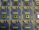
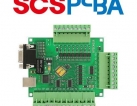
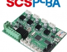
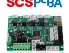
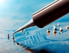
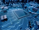
PCB Depanelization Tools
China, Shanghai City, Shanghai - view exact location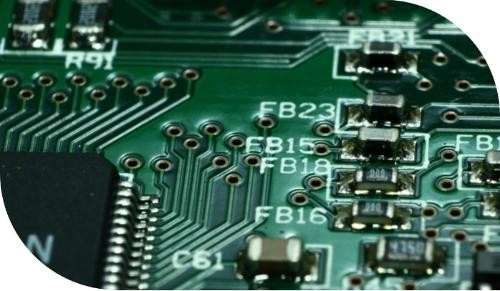
Category
Product Information
Order volume from: On request
Delivery terms: Pickup
Description
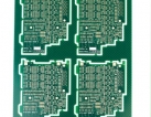
PCB depanelization is a crucial process involved in the manufacturing of electronic assemblies within the PCB and surface mount technology (SMT) industry. In order to optimize the efficiency of production lines and enhance overall throughput, the design of printed circuit boards often includes multiple interconnected smaller boards known as panels or multi-blocks. These panels collectively form a complete PCB cluster that will ultimately be integrated into the final product.
The depanelization process involves the separation or breaking down of the large panel into individual PCBs. The precise timing of this step varies depending on the specific product requirements. It can occur immediately after the SMT process, following the in-circuit test (ICT), or even after the soldering of through-hole components. In some cases, depanelization takes place just before the final assembly of the printed circuit board assembly (PCBA) into its respective enclosure.
By efficiently depanelizing the large panel into smaller PCBs, manufacturers are able to streamline the production process and ensure the successful integration of electronic components into the final product.