Business
 Business
 Commercial Property
 Investment
 Franchise
 Equipment
 Heavy Equipment
 Tenders
 Services
 Goods
Goods
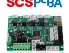
One-Stop OEM EMS Custom PCB PCBA SMT DIP Test
China, Beijing City, Beijing - view exact location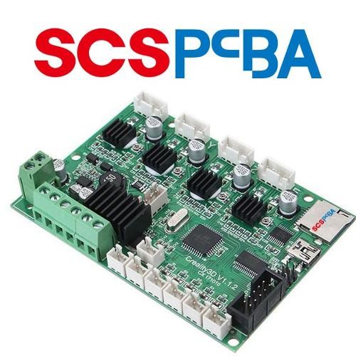
Category
Product Information
Order volume from: On request
Delivery terms: Pickup
Description
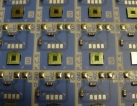
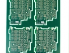
PCB depanelization is a crucial process step in the electronics manufacturing industry. It plays a significant role in increasing the productivity of large-scale assembly of electronic devices, particularly in the production lines of printed circuit boards (PCBs) and surface mount technology (SMT).
To optimize efficiency, PCBs are often designed as a cluster consisting of multiple smaller individual printed circuit boards. These smaller boards, known as panels or multi-blocks, are later utilized in the final product. Prior to their integration, the large panel undergoes a depanelization process.
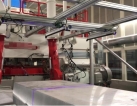
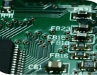
The depanelization procedure can occur at various stages, depending on the specific product requirements. It may take place immediately after the SMT process, or after conducting an in-circuit test (ICT). Alternatively, depanelization can happen after soldering the through-hole components or even just prior to the final assembly of the printed circuit board assembly (PCBA) in its enclosure.
By carrying out this crucial step, PCB depanelization ensures the smooth and efficient production of electronic devices, enabling the seamless integration of multiple smaller circuit boards into the final product.