Business
 Business
 Commercial Property
 Investment
 Franchise
 Equipment
 Heavy Equipment
 Tenders
 Services
 Goods
Goods
5372
China, Shanghai City, Shanghai - view exact location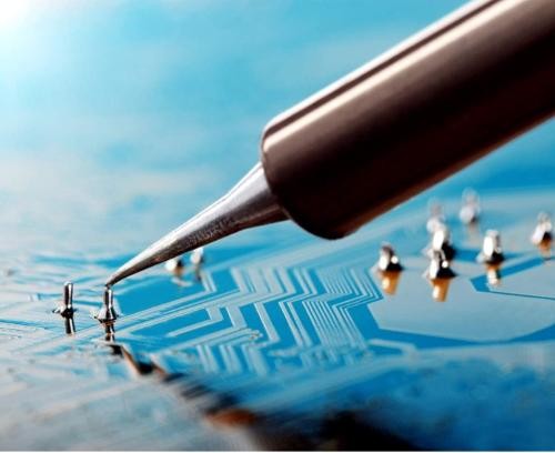
Product Information
Order volume from: On request
Delivery terms: Pickup
Description
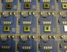
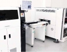
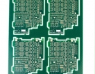
PCB depanelization is a crucial process in the electronics manufacturing industry, particularly in large-scale assembly. It involves breaking down a cluster of printed circuit boards (PCB) into smaller individual boards, known as panels or multi-blocks. These smaller boards are then utilized in the final product, enhancing the throughput of PCB and surface mount production lines.
The depanelization process typically occurs at various stages depending on the specific product requirements. It can be implemented immediately after the surface mount technology (SMT) process, following in-circuit testing (ICT), after soldering through-hole components, or just before the final assembly of the printed circuit board assembly (PCBA) within the enclosure.
By depanelizing the PCB cluster, manufacturers can optimize production efficiency and effectively manage the manufacturing workflow. This ensures seamless integration of the printed circuit boards into the final product, meeting the industry's demands for high-quality electronic assemblies.