Business
 Business
 Commercial Property
 Investment
 Franchise
 Equipment
 Heavy Equipment
 Tenders
 Services
 Goods
Goods
3727
China, Beijing City, Beijing - view exact location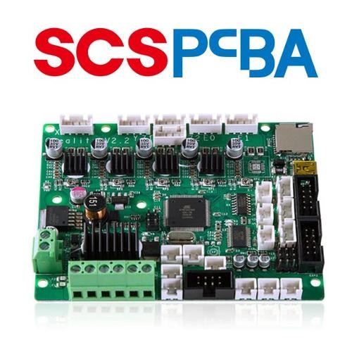
Category
Product Information
Order volume from: On request
Delivery terms: Pickup
Description
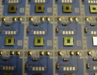
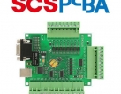
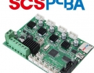
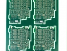
PCB depanelization is a critical step in the electronics manufacturing industry, specifically in the production of large-scale assemblies. In order to optimize the efficiency of PCB and SMT production lines, engineers often design printed circuit boards to consist of multiple smaller individual boards, collectively known as a panel or multi-block. These panels are then subjected to a depanelization process to separate them into individual PCBs.
Depanelization typically takes place at various stages of the manufacturing process, depending on the specific requirements of the final product. It can occur right after the SMT process, after the in-circuit test (ICT), after the soldering of through-hole components, or even just before the final assembly of the PCBA in the enclosure.
By breaking down the larger panel into individual PCBs, the manufacturing process becomes more streamlined, allowing for improved throughput and efficiency. PCB depanelization plays a crucial role in ensuring the successful assembly of electronics and is an essential step in the production of high-quality, reliable products.