Business
 Business
 Commercial Property
 Investment
 Franchise
 Equipment
 Heavy Equipment
 Tenders
 Services
 Goods
Goods
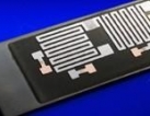
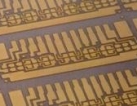
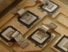
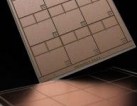
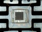
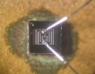
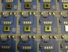
1. DCB ( Direct Ceramic Bond) Substrate
Germany, Berlin Land, Berlin - view exact location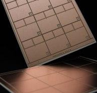
Product Information
Order volume from: On request
Delivery terms: Pickup
Description
The DBC (Direct Bonded Copper) technique is a specialized process that involves directly bonding copper foil with al2o3 or AlN (on one or both sides) at high temperatures. This results in a super-thin DBC substrate that offers outstanding electrical isolation, high thermal conductivity, excellent solderability, and strong bonding strength. Similar to a PCB, this substrate can be structured to create etched wiring and is capable of handling high current loads. DBC ceramic substrates are now widely used in the construction and interconnection techniques of high power semiconductor electronic circuits. They have also become the foundation for chip on board technology, which represents the packaging trend of this century.Specification:- Metallization thickness: 25 ±10um- Nickel thickness: 2~10um- Pin full strength: average of 4200kgf/cm2 (at Φ3.0mm pin)