Business
 Business
 Commercial Property
 Investment
 Franchise
 Equipment
 Heavy Equipment
 Tenders
 Services
 Goods
Goods
0120
USA, New Jersey State, West New York - view exact location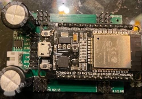
Category
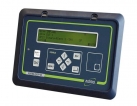
Product Information
Order volume from: On request
Delivery terms: Pickup
Description
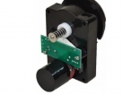
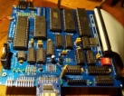
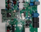
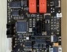
PCB depanelization is an essential process in the electronics industry that is used during the production of large-scale assembly of electronics. As part of the manufacturing process to enhance the efficiency of PCB and SMT production lines, printed circuit boards are often composed of multiple smaller individual boards that will be integrated into the final product. These interconnected boards, known as panels or multi-blocks, are then depanellated or broken apart as a crucial step.
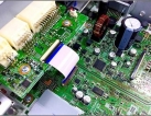
The exact timing of the depanelization process varies depending on the specific requirements of the product being manufactured. In some cases, the depanelization occurs immediately after the SMT process, while in others, it may take place after the in-circuit test (ICT) or after soldering through-hole components. In some instances, depanelization even occurs just prior to the final assembly of the PCBA (Printed Circuit Board Assembly) in its enclosure.
By employing the depanelization process, production lines can boost the overall throughput of PCB and SMT operations, facilitating the smooth integration of the smaller boards into the final product. This meticulous process ensures the efficient and accurate production of electronics, meeting the industry's high standards for quality and reliability.