5869
USA, New Jersey State, West New York - view exact locationProduct Information
Order volume from: On request
Delivery terms: Pickup
Description
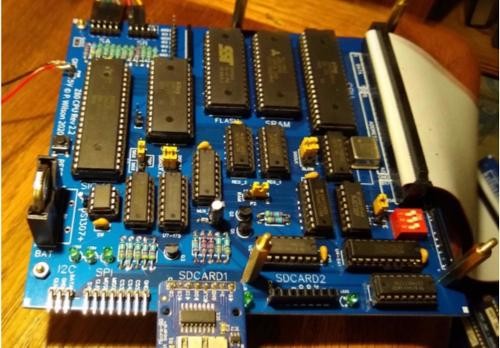
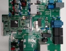
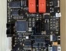
PCB depanelization is a crucial step in the electronics manufacturing industry. It involves separating large-scale printed circuit board (PCB) assemblies into smaller individual boards to optimize production efficiency. This process is particularly beneficial for increasing the throughput of PCB and surface mount technology (SMT) production lines.
To achieve this, designers often create PCB clusters, also known as panels or multi-blocks, which consist of multiple smaller boards that will eventually be used in the final product. These clusters are then depanellated or broken apart during the manufacturing process. The timing of depanelization can vary depending on the product being produced. It can take place after the SMT process, after the in-circuit test (ICT), after the soldering of through-hole components, or even just before the final assembly of the PCB assembly (PCBA) into its enclosure.
By incorporating PCB depanelization into the production workflow, manufacturers can enhance overall efficiency and productivity while ensuring the successful creation of electronic products.

 Business
