Business
 Business
 Commercial Property
 Investment
 Franchise
 Equipment
 Heavy Equipment
 Tenders
 Services
 Goods
Goods
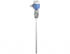
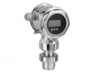
Sonelastic HZ
Brazil, Rio de Janeiro state, Rio de Janeiro - view exact location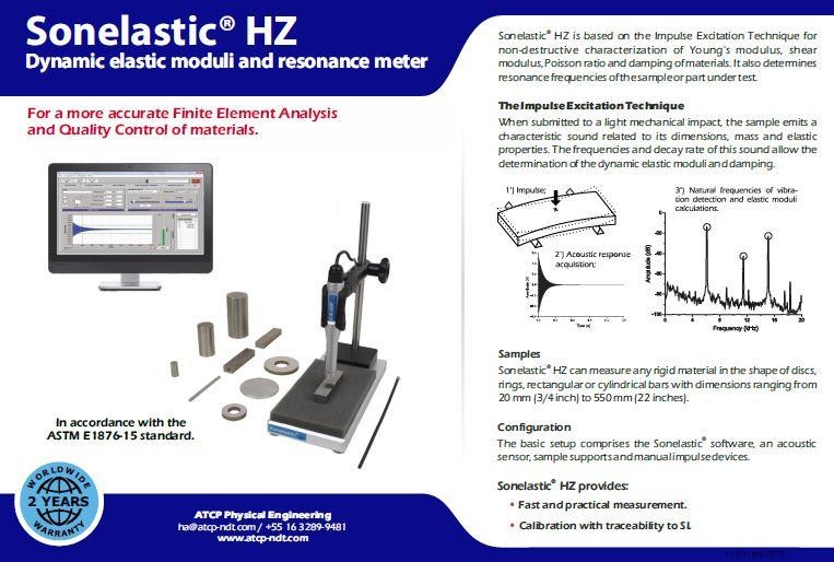
Category
- Instruments For Measuring, Temperature Control >> Instrumentation >> Goods >> Thermometers, Pyrometers, Thermal Imagers
- Instruments For Measuring, Temperature Control >> Instrumentation >> Goods >> Temperature Sensors
- Instruments For Measuring, Temperature Control >> Instrumentation >> Goods >> Resistance Thermometers
Product Information
Order volume from: On request
Delivery terms: Pickup
Description
Product Description:
The Wafer Measuring System is a cutting-edge solution designed specifically for the wafer industry. It offers a range of powerful features and capabilities to ensure accurate and precise measurements.
Here are the key features of the Wafer Measuring System:
1. Measurement Technology: Utilizes a displacement-type non-contact coaxial laser displacement sensor for precise measurements.
2. Gantry Movement Mechanism: Equipped with a linear motor high precision gantry movement mechanism, ensuring smooth and accurate movements during measurements.
3. Compatibility: Designed to measure both polished and unpolished, transparent and non-transparent wafers, making it versatile for various applications.
4. Wafer Size Compatibility: Supports wafer samples ranging from 1-8 inches in diameter, with the option to extend the capability to accommodate larger 300mm (12 inch) products.
5. Enhanced Stability: Incorporates a coplanar air floating mobile bearing system, ensuring the wafer sample moves with exceptional flatness and smoothness, minimizing any potential disturbances.
6. Measurement Range: Capable of measuring the thickness of a wafer ranging from 10 micrometers to 20 millimeters, accommodating a wide range of wafer thicknesses.
7. Maximum Scanning Speed: Offers a fast scanning speed of up to 1 micrometer per second, allowing for efficient and time-saving measurements.
8. Measurement Parameters: Provides comprehensive measurement parameters, including thickness, total thickness variation (TTV), local thickness variation (LTV), total indicator reading (TIR), sori, taper, bow, and warp. It adheres to industry standards for these measurements.
The Wafer Measuring System is an indispensable tool for the wafer industry, enabling precise and accurate measurements of various wafer properties. Whether for research and development or quality control purposes, this system offers reliability, versatility, and efficiency in wafer measurements.