Unternehmen
 Geschäft
 Gewerbeimmobilien
 Investition
 Franchise
 Ausrüstung
 Sonderausstattung
 Ausschreibungen
 Dienstleistungen
 Waren
Waren
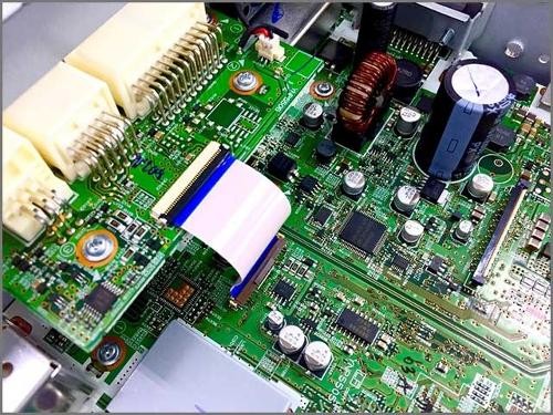
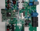
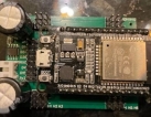
Batterieschutzschaltungsmodul (PCBA) - Elektronik Surfa
USA, Illinois Staat, Chicago - siehe genauen StandortKategorie
Produktinformation
Auftragsvolumen ab: Auf Anfrage
Lieferbedingungen: Aufsammeln
Auftragsvolumen ab: Auf Anfrage
Lieferbedingungen: Aufsammeln
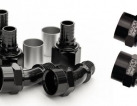
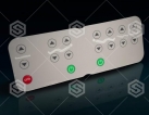 Geprägtes Grafikfeld
Preis auf Anfrage
Die Türkei,
Marmara Region, Istanbul
Geprägtes Grafikfeld
Preis auf Anfrage
Die Türkei,
Marmara Region, Istanbul
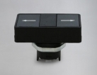 Doppeltaster schwarz-schwarz mit Anzeige EPD/F
Preis auf Anfrage
Slowenien,
Osrednjeslovenska Regia, Ljubljana
Doppeltaster schwarz-schwarz mit Anzeige EPD/F
Preis auf Anfrage
Slowenien,
Osrednjeslovenska Regia, Ljubljana
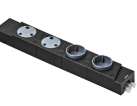 Schräg
Preis auf Anfrage
Jamaika,
Provinz Gauteng, Johannesburg
Schräg
Preis auf Anfrage
Jamaika,
Provinz Gauteng, Johannesburg
 Optima
Preis auf Anfrage
Jamaika,
Provinz Gauteng, Johannesburg
Optima
Preis auf Anfrage
Jamaika,
Provinz Gauteng, Johannesburg
 G-Linie Ultra 860 und 960
Preis auf Anfrage
Deutschland,
Berlin Land, Berlin
G-Linie Ultra 860 und 960
Preis auf Anfrage
Deutschland,
Berlin Land, Berlin
 Maßgeschneiderte Montagemaschinen
Preis auf Anfrage
UK,
Groß-London, London
Maßgeschneiderte Montagemaschinen
Preis auf Anfrage
UK,
Groß-London, London
 5869
Preis auf Anfrage
USA,
New Jersey Staat, West New York
5869
Preis auf Anfrage
USA,
New Jersey Staat, West New York
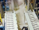
 Zoom-Teilen: Bestückung einer gedruckten Schaltungskarte ohne Unterbrechung
Preis auf Anfrage
USA,
Illinois Staat, Chicago
Zoom-Teilen: Bestückung einer gedruckten Schaltungskarte ohne Unterbrechung
Preis auf Anfrage
USA,
Illinois Staat, Chicago
 0120
Preis auf Anfrage
USA,
New Jersey Staat, West New York
0120
Preis auf Anfrage
USA,
New Jersey Staat, West New York
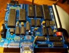
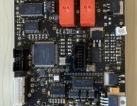 ARM Multilayer PCB Assembly Prototyp - Kundenspezifische PCBA SMT
Preis auf Anfrage
USA,
New Jersey Staat, West New York
ARM Multilayer PCB Assembly Prototyp - Kundenspezifische PCBA SMT
Preis auf Anfrage
USA,
New Jersey Staat, West New York